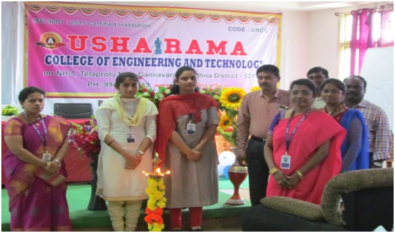
WORKSHOP ON PCB DESIGN in Dec 2019
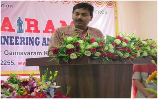
Two day (19 DEC 2019 & 20 DEC 2019) training is conducted for II DECE students on PCB Design at Usha Rama College of Engineering & Technology, Telaprolu. Mr. V.GOVIND RAO of MICROLINK had accompanied students for two days.
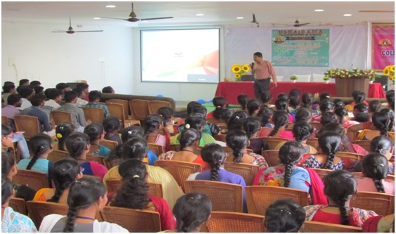
No. Of Students participated: 170
Training Summary:
The training comprises of four sessions Theory class followed by Laboratory completely for two days. The students are taught on the Introduction to circuit designing, Introduction to PCB Design, Design transfer to the PCB and design rule check, Component placement and shielding and Routing PCB Layout Routing and Grounding.
Finally students had been able to understand the performance and maintenance of PCB.